1Overview
The Model 866-M is a compact-size frequency synthesizer for the generation of accurate and stable frequency signals in both CW and pulse form, covering a frequency range of 1 MHz to 40 GHz, with a fast-switching time of 50 µs, an output power of -20 to +25 dBm. The device shows excellent phase noise performance, e.g., at 10 GHz and 20 kHz offset -127 dBc/Hz is measured.
The synthesizer is in a very compact flange-mountable form of 6.5 x 2.4 x 1 inches [165 x 60 x 26 mm], weighs less than 1.3 lbs, and consumes less than 23 W and is only passively cooled. The Ethernet communication port is used for remote connection to a PC for control over GUI software using standard SCPI commands.
The module can receive and provide external references of 100 MHz or 1 GHz. Multiple units can be phase synchronized with one unit acting as the master and the others as slaves, to implement multi-channel phase-coherent outputs.
The product is suitable for many applications: as low phase noise system clock or reference sources, in the multi-channel phase-coherent configurations for radar, EW, quantum computing, etc.
2Key Features & Applications
Features
- Small size flange-mount module
- CW and pulse modulation
- Low power consumption as low as 23 W, passive cooling
Applications
- System clock source
- Multi-channel phase-coherent configurations for radar signal generation and testing
- Spectroscopy
3Frequency & Output Power
Signal Specifications
| Parameter | Min | Typical | Max | Note |
|---|---|---|---|---|
| Frequency Range | 1 MHz | 40 GHz | ||
| Frequency Resolution | 0.001 Hz | GUI SW setting resolution | ||
| Phase Adjustment Range | 0 deg | 360 deg | ||
| Phase Resolution | 0.1 deg | |||
| Switching Speed | 500 µs 50 µs | 85 µs | Option FS |
Frequency Reference
| Parameter | Min | Typical | Max | Note |
|---|---|---|---|---|
| Internal reference frequency | 100 MHz | |||
| Calibrated accuracy of int. reference | ±30 ppb | Calibrated at 23 ± 3 °C | ||
| Temperature stability (0 to 50 °C) | ±100 ppb | |||
| Aging 1st year | 500 ppb | |||
| Aging per day | 5 ppb | After 30 days operation | ||
| Warm-Up time | 5 min | |||
| Reference frequency input | 100 MHz, 1 GHz | |||
| Reference input level (100 MHz 1 GHz) | -5 dBm -5 dBm | +10 dBm +10 dBm | ||
| Reference input impedance | 50 Ω | |||
| Reference frequency output | 100 MHz, 1 GHz | 100 MHz reference out not possible when using 1 GHz external reference | ||
| Output power (100 MHz 1 GHz) | 0 dBm -1 dBm | 5 dBm 5 dBm | ||
| Reference output impedance | 50 Ω | |||
| Multi-Channel configurability | ||||
| Recommended configuration | One master and multiple slave units are synchronized by the common 1 GHz reference from the master unit | |||
| Relative phase stability among the multi-channels (phase coherence) | 15 mrad | @ 5 GHz over 5 hours | ||
Level Performance
| Parameter | Min | Typical | Max | Note |
|---|---|---|---|---|
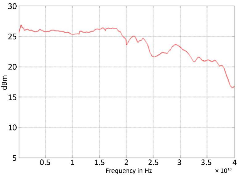
| Output power level | See plot below | |||
| < 1 GHz | -10 dBm | 24 dBm | ||
| 1 GHz to 18 GHz | -10 dBm | 25 dBm | ||
| 18 GHz to 23 GHz | -10 dBm | 23 dBm | ||
| 23 GHz to 32 GHz | -20 dBm | 21 dBm | ||
| 32 GHz to 40 GHz | -20 dBm | 17 dBm | ||
| Power resolution | 0.5 dB |
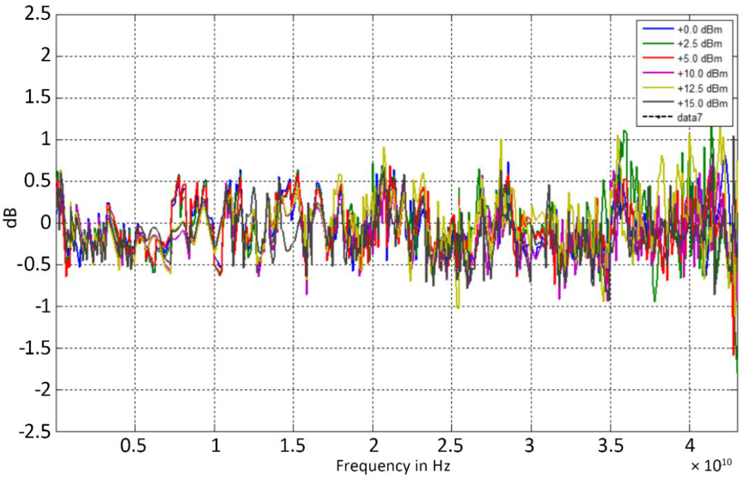
Level Uncertainty
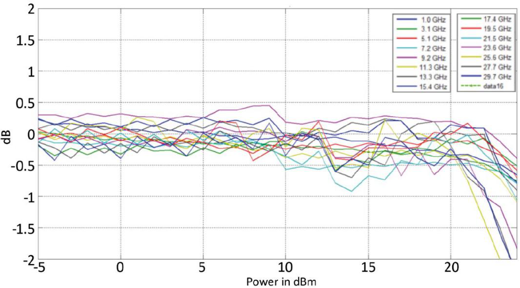
| Parameter | Min | Typical | Max | Note |
|---|---|---|---|---|
| Power level uncertainty | See plots below | |||
| <15 GHz | 0.5 dB | 1.0 dB | 0 to 15 dBm | |
| 15 GHz to 35 GHz | 1.0 dB | 1.5 dB | 0 to 15 dBm | |
| 35 GHz to 40 GHz | 1.0 dB | 2.0 dB | 0 to 15 dBm |
Reverse Power Protection and VSWR
| Parameter | Min | Typical | Max | Note |
|---|---|---|---|---|
| Output impedance VSWR | 50 Ω 1.7 | |||
| Reverse power protection | ||||
| DC voltage | 7 V | |||
| RF power | 23 dBm |
4Phase Noise & Spectral Purity
Phase Noise
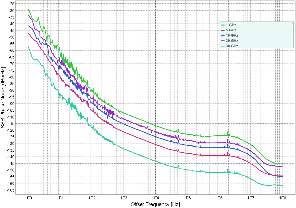
| Parameter | Min | Typical | Max | Note |
|---|---|---|---|---|
| SSB Phase noise at 1 GHz | See plot below | |||
| at 10 Hz from carrier | -87 dBc/Hz | -80 dBc/Hz | ||
| at 1 kHz from carrier | -130 dBc/Hz | -125 dBc/Hz | ||
| at 100 kHz from carrier | -145 dBc/Hz | -140 dBc/Hz | ||
| at 10 MHz from carrier | -155 dBc/Hz | -150 dBc/Hz | ||
| SSB Phase noise at 10 GHz | See plot below | |||
| at 10 Hz from carrier | -66 dBc/Hz | -60 dBc/Hz | ||
| at 1 kHz from carrier | -113 dBc/Hz | -108 dBc/Hz | ||
| at 100 kHz from carrier | -129 dBc/Hz | -124 dBc/Hz | ||
| at 10 MHz from carrier | -138 dBc/Hz | -133 dBc/Hz |
Spectral Purity
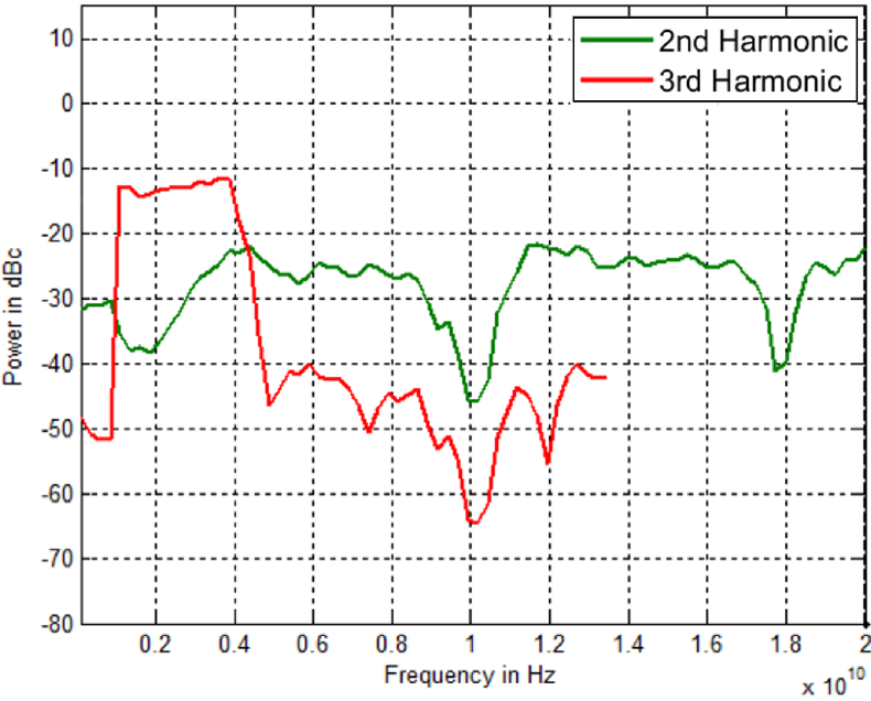
| Parameter | Min | Typical | Max | Note |
|---|---|---|---|---|
| Harmonics | At 10 dBm; See plot below | |||
| < 1 GHz | -30 dBc | -25 dBc | ||
| 1 GHz to 4 GHz | -15 dBc | -10 dBc | ||
| 4 GHz to 20 GHz | -25 dBc | -15 dBc | ||
| 20 GHz to 40 GHz | -20 dBc | |||
| Sub-harmonics | At 10 dBm | |||
| < 4 GHz | -80 dBc | -70 dBc | ||
| 4 GHz to 20 GHz | -70 dBc | -75 dBc | ||
| 20 GHz to 40 GHz | -55 dBc | -40 dBc | ||
| Non-harmonic spurious | >10 kHz offset | |||
| < 1 GHz | -55 dBc | -50 dBc | ||
| 1 GHz to 20 GHz | -70 dBc | -60 dBc | ||
| 20 GHz to 40 GHz | -60 dBc |
5Sweeping & Trigger
Sweeping Capability
| Parameter | Min | Typical | Max | Note |
|---|---|---|---|---|
| Sweep parameters | Frequency, power, list | |||
| Sweep type | Linear, logarithmic, random | |||
| Step Time | 500 µs 50 µs | 20 s 20 s | Option FS | |
| Timing resolution | 10 ns | |||
| Timing accuracy per point | 20 ns | |||
| Generalized list sweep | Allows for individual setting of frequency, power, step-time, and off-time for each point. | |||
Trigger (TRIG)
| Parameter | Min | Typical | Max | Note |
|---|---|---|---|---|
| Trigger types | Continuous; Single (point); Gated; Gated direction | |||
| Trigger source | External; Ethernet | |||
| Trigger modes | Continuous free run; Trigger and run; Reset and run | |||
| External trigger latency | 140 ns | |||
| External trigger uncertainty | 20 ns | |||
| External trigger delay | 0 s | 20 s | Settable | |
| External delay resolution | 10 ns | |||
| Trigger modulo | 1 | 255 | Execute only on Nth trigger event | |
| Trigger polarity | Rising; Falling | |||
| External trigger input threshold | 0.85 V | 0.9 V | 0.95 V | TTL compatible |
| External trigger input voltage range | -0.5 V | +5.5 V | TTL compatible | |
| External trigger input hysteresis | 60 mV | |||
6Modulation
Modulation Capability
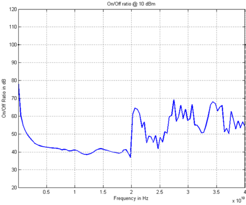
| Parameter | Min | Typical | Max | Note |
|---|---|---|---|---|
| Pulse modulation | ||||
| Modulation source | Internal; External | Trigger port can be reconfigured as external modulation port | ||
| On/off ratio < 1 GHz 1 GHz to 20 GHz 20 GHz to 27 GHz 27 GHz to 40 GHz | 50 dB 30 dB 35 dB 45 dB | 60 dB 40 dB 45 dB 55 dB | At 10 dBm; See plot below. | |
| Repetition frequency | DC | 10 MHz | ||
| Pulse width | 30 ns | 20 s | ||
| Pulse rise/fall time | 9 ns | |||
| Pulse train length | 1 | 4096 | ||
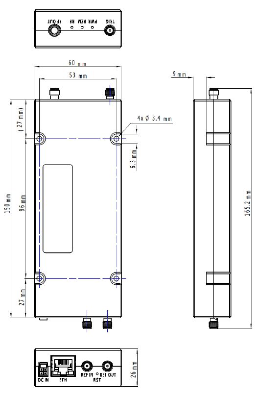
7Mechanical & Connectors
Dimensions & Weight
| Dimensions / Weight | Including Connectors |
|---|---|
| W x L x H | 6.5 x 2.4 x 1” [165 x 60 x 26 mm] / 1 lb [0.45 kg] |
Installation Instructions
The module relies on passive cooling. It is mandatory to mount the device on a heatsinking surface. Make sure the synthesizer operates under the conditions specified in the datasheet. Otherwise, the thermal protection will turn off the RF output.
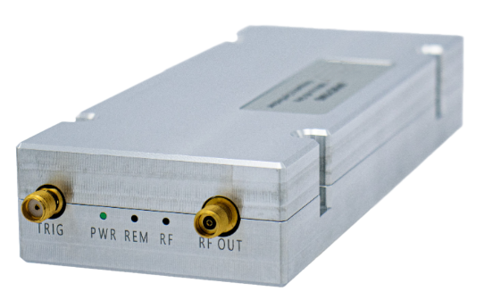
Front Panel
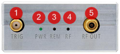
| Label | Type | Description |
|---|---|---|
| 1. TRIG | SMA | Trigger Signal input |
| 2. PWR | LED | Power ON/OFF indicator |
| 3. REM | LED | Remote connection status indicator |
| 4. RF | LED | RF output ON/OFF indicator |
| 5. RF OUT | 2.92 mm | RF output |
Rear Panel
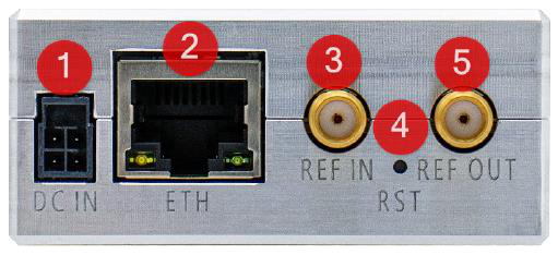
| Label | Type | Description |
|---|---|---|
| 1. DC IN | 1053141104 (Molex) | DC input (see also chapter “Power Connector Assembly”) |
| 2. ETH | RJ-45 | Ethernet port |
| 3. REF IN | SMA | Reference Signal input |
| 4. RST | Button | Reset Button |
| 5. REF OUT | SMA | Reference Signal output |
Power Connector Assembly
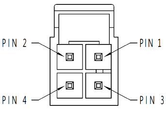
| Pin | Assignment |
|---|---|
| 1 | DC Supply (see also “Power requirements”) |
| 2 | GND |
| 3 | DC Supply (see also “Power requirements”) |
| 4 | GND |
The power connector is a 4 pin, 2.50 mm spaced double-row header. BNC recommends Molex manufactured receptacles 1053081204 and contacts 1053002200 with TPA retainer 1053252002 from its Nano-Fit series.
Reset Functionality
The reset functionality of the device can be used if the device has a wrong configured IP address and cannot be found in the local area network anymore. While pressing the reset button (>2 s), the device will be reconfigured to auto IP addressing mode (DHCP/Zero-conf) and restarts itself. After the device is up and running again, it gets a new IP address and can be discovered by the BNC Signal Generator UI.
8General Characteristics
| Parameter | Specification |
|---|---|
| Remote Programming Interfaces | Ethernet |
| Control language | SCPI Version 1999.0 |
| Power requirements | 24±6 VDC; 23 W maximum |
| Mains adapter supplied | 100-240 VAC in / 24 V, 2.7 A DC out |
| Storage temperature range | -40 to 70 °C |
| Operating temperature range | 0 to 45 °C, non-condensing |
| Operating and storage altitude | up to 15,000 feet |
| Safety/EMC | complies with applicable Safety and EMC regulations and directives |
| Recommended calibration cycle | 24 months |
9Ordering Information
| Host Model | Product | Description |
|---|---|---|
| 866-M | 866-M | 40 GHz wideband frequency synthesizer module (with AC adapter) |
| 866-M | Option FS | Fast Switching |
10Applications
- System clock source
- Multi-channel phase-coherent configurations for radar signal generation and testing
- Spectroscopy
The product is suitable for many applications: as low phase noise system clock or reference sources, in the multi-channel phase-coherent configurations for radar, EW, quantum computing, etc.