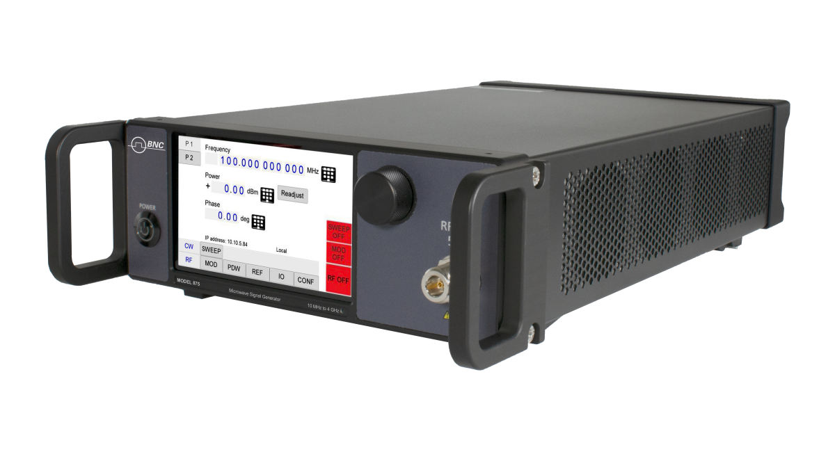
Model 875 10 MHz to 40 GHz Multi-Channel Vector Signal Generator
A vector-modulated signal generator covering 10 MHz to 40 GHz continuously, with an internal I/Q modulator, deep waveform memory, and real-time Pulse Descriptor Word playback for radar and EW emulation. Phase-coherent across up to four channels, switching down to 200 ns.
Specifications reproduced from Model 875 datasheet V132 (dc-61704202). Warranted at 23 ±5 °C after 30-minute warm-up unless stated.
1Introduction
The Model 875 is an ultra-fast-switching, vector-modulated signal generator series covering continuous frequency ranges from 10 MHz (100 kHz with option 100K) to 4, 6, 12, 20, or 40 GHz, respectively, with 0.001 Hz resolution and 400 MHz RF modulation bandwidth.
The Model 875 is the corresponding multi-channel product series, up to 4 channels per device. This specification applies to single channel models as well as to the independent channels of multi-channel models.
A high performance internal I/Q modulator enables customized waveforms as modulation signals and supports a variety of modulation schemes including avionics modulation. The digital I/Q modulator ensures excellent carrier suppression and a very high image suppression. The standard Model 875 enables ultra-fast CW frequency sweeping, chirping, intra-pulse modulation, and pulse shaping with very low phase noise. Multi-channel models exhibit exceptionally high phase stability between channels synchronized by the same common reference.
Among others, the following use cases are supported:
Upload multiple formats of I/Q data into the Model 875 memory. A Model 875 GUI supports data formats from various vendors. The internal RAM can store up to 512 MS (32 bits per I/Q sample) of I/Q data. The Model 875 internal AWG can play selected sections of the RAM upon a user trigger.
Use the Model 875 to synthesize and play predefined digital modulation formats (option IVM).
Use the analog I & Q inputs (option AIQ) with up to 50 MHz analog bandwidth.
Use the FCP interface (option FCP) to: live stream digital I/Q data; instantaneously switch between pre-loaded I/Q data segments; control ultra-fast frequency hopping (additionally, option UFS required).
All models operate with an ultra-stable temperature-compensated frequency reference (OCXO) that can be phase-locked to an external reference. The compact device can be controlled by the touch display and a PC user interface.
Definitions
The specifications describe the warranted performance of the instrument for 23 ±5 °C after a 30-minute warm-up period, unless otherwise stated.
Min/Max: Parameter range that is guaranteed by product design and/or production tested. Warranted performance specifications include guard-bands to account for the expected statistical performance distribution, measurement uncertainties, and changes in performance due to environmental conditions.
Typical: Expected mean values, not warranted performance.
Features
Excellent phase noise
Ultra-fast switching
Ultra-high I/Q data rates, deep internal memory
Various digital modulation supported
Applications
Arbitrary I/Q waveform
Radar signal simulation
Receiver testing
Avionic modulation emulation
High speed antenna testing
2Available Options
The 875 is configured from hardware options, software licenses, and accessories. See Ordering Information for the full option list and applicability per model. Key options referenced throughout these specifications:
Option
Description
100K
Frequency range extension to 100 kHz
LN / LN+
Enhanced close-in phase noise & frequency stability (LN+ adds further enhanced long-term frequency stability)
PE / PE2 / PE4
Mechanical and electronic step attenuators for extended level range (down to -90 dBm / -120 dBm / electronic)
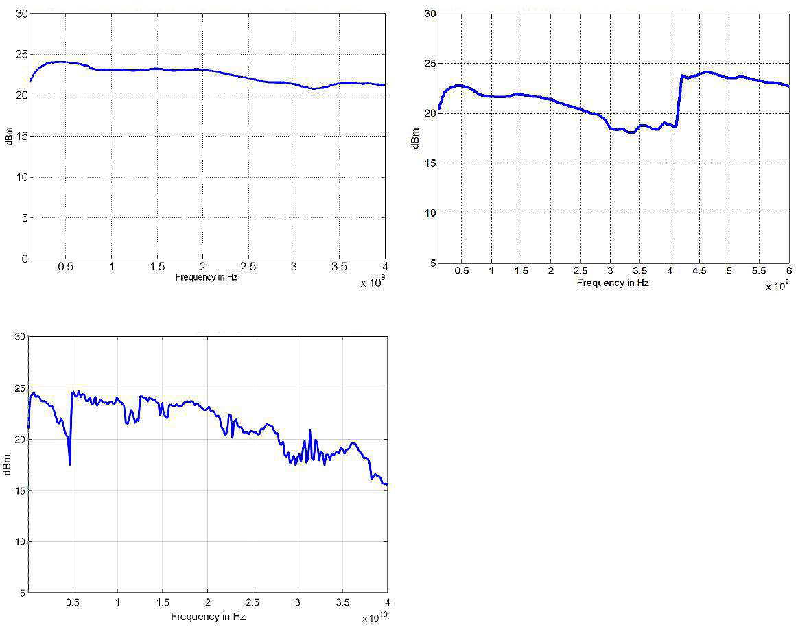
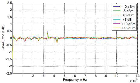
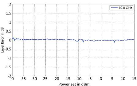
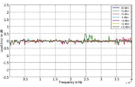
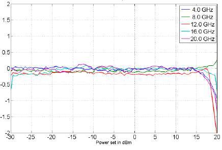
Figure 4: Power Level Accuracy, 875-12 (level error vs frequency).Figure 5: Power Level Accuracy, 875-12 (level error vs power set).Figure 6: Power Level Accuracy, 875-40.Figure 7: Power Level Accuracy, 875-20.
Frequency
Typical
Max
Note
< 4 GHz
0.25 dB
0.7 dB
> -20 dBm
4 to 6 GHz
0.3 dB
1.0 dB
> -20 dBm
6 to 20 GHz
0.3 dB
1.3 dB
> -20 dBm
20 to 40 GHz
0.3 dB
1.5 dB
> -20 dBm
< 4 GHz
0.3 dB
0.8 dB
Pmin to -20 dBm
4 to 6 GHz
0.35 dB
1.2 dB
Pmin to -20 dBm
6 to 20 GHz
0.4 dB
1.4 dB
Pmin to -20 dBm
20 to 40 GHz
0.5 dB
1.6 dB
Pmin to -20 dBm
Reverse Power Protection and VSWR
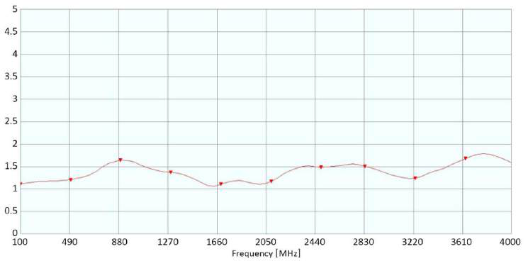
Figure 8: Typical VSWR, 875-04.
Parameter
Typical
Max
Note
Reverse power protection — DC voltage
±10 V
Reverse power protection — RF power
+26 dBm
Output Impedance
50 Ω
VSWR
1.8
See performance curves
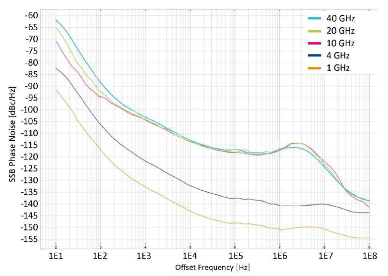
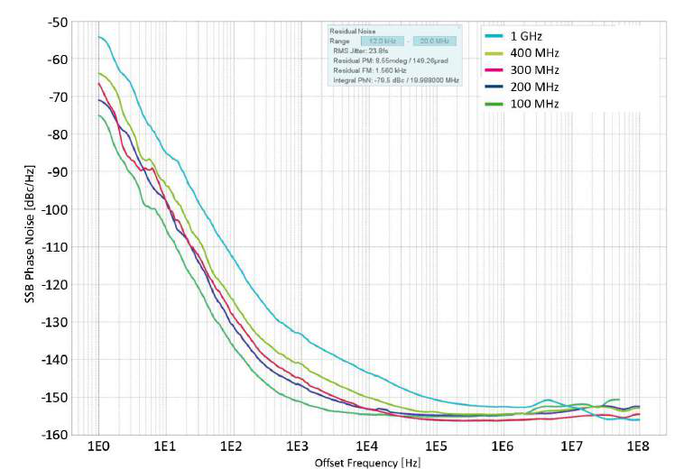
7Phase Noise
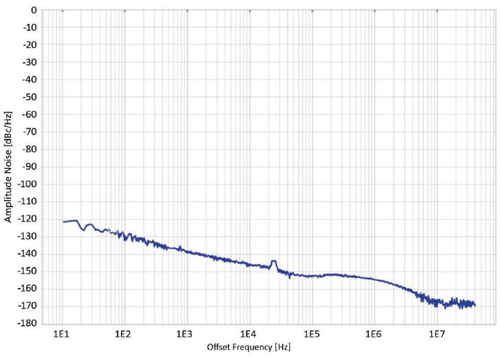
Figure 10: SSB Phase Noise Performance, 875-20/40, CW without option LN, Pout = +10 dBm.Figure 11: SSB Phase Noise Performance, 875-XX, low-frequency CW without option LN, Pout = +10 dBm.Figure 12: Amplitude Noise, 2 GHz, Pout = +10 dBm.
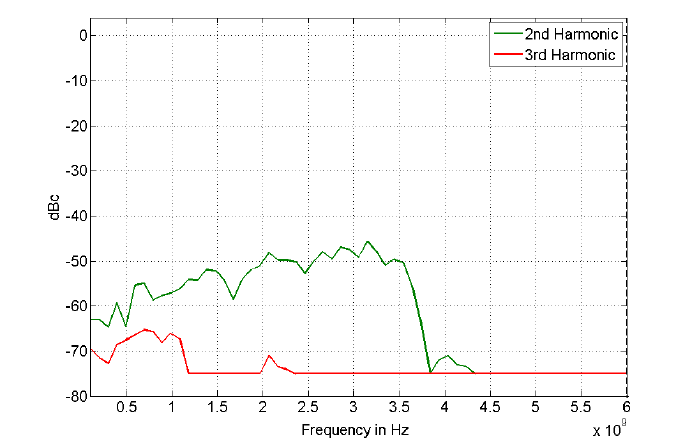
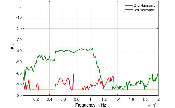
Figure 13: 875-06 Harmonic Performance at Pout = 0 dBm.Figure 14: 875-20 Harmonic Performance at Pout = 0 dBm.
Harmonics at 0 dBm
Model / Range
Typical
Max
875-04
0.01 to 2 GHz
-55 dBc
-48 dBc
2 to 4 GHz
-45 dBc
-40 dBc
875-06
0.01 to 4 GHz
-45 dBc
-40 dBc
4 to 6 GHz
-35 dBc
-30 dBc
875-12
0.01 to 4 GHz
-45 dBc
-40 dBc
4 to 7 GHz
-35 dBc
-30 dBc
7 to 12 GHz
-55 dBc
-50 dBc
875-20
0.01 to 4.5 GHz
-50 dBc
-40 dBc
4.5 to 10.5 GHz
-40 dBc
-30 dBc
> 10.5 GHz
-55 dBc
-48 dBc
875-40
0.01 to 4.5 GHz
-50 dBc
-45 dBc
4.5 to 20 GHz
-35 dBc
-30 dBc
> 20 GHz
-35 dBc
-30 dBc
Non-Harmonic Spurious
At 0 dBm output, > 10 kHz offset.
Range
Typical
Max
< 1.2 GHz
-90 dBc
-75 dBc
1.2 to 2.5 GHz
-80 dBc
-70 dBc
2.5 to 4 GHz
-80 dBc
-50 dBc
4 to 12 GHz
-70 dBc
-50 dBc
12 to 20 GHz
-60 dBc
-50 dBc
> 20 GHz
-55 dBc
-50 dBc
9Sweeping Capability
Parameter
Min
Typical
Max
Note
Sweep Type
Digital sweep in discrete steps
Automatic Level Control (ALC) Mode
OFF
Power Level Uncertainty
0.5 dB
1 dB
875-04
TBD
TBD
875-06/12/20/40
Frequency & Amplitude Switching Transient Time (can be blanked during "Delay Time")
500 µs
1 µs
875-04 Option UFS
2 µs
875-20, 875-40 Option UFS
Sweep Spacing
Linear
Sweep Shape
Sawtooth
Sweep Parameters
Frequency, Power
Sweep Range
Full specified range
Frequency sweep
-20 to +15 dBm
Power sweep, 875-04
Step Size Setting Resolution
0.001 Hz
Frequency sweep
0.01 dB
Power sweep
Dwell Time Setting Range
500 µs
34.35 s
800 ns
34.35 s
875-04 Option UFS
TBD
34.35 s
875-20, 875-40 Option UFS
Delay (off) Time Setting Range
200 ns
34.35 s
875-04
200 ns
34.35 s
875-20, 875-40
Dwell/Delay Time Resolution
8 ns
Sweep Count
Infinite, 1 to 1 M
Trigger Type
Normal (full sweep), Point (one step)
Check with BNC support
Trigger Parameters
See Trigger Capability
Retrigger Setup Time
200 ns
External Trigger Event to RF Output Delay
TBD
875-04, Option UFS
TBD
875-20, 875-40, Option UFS
10Phase Coherence
Phase-Coherent Modes
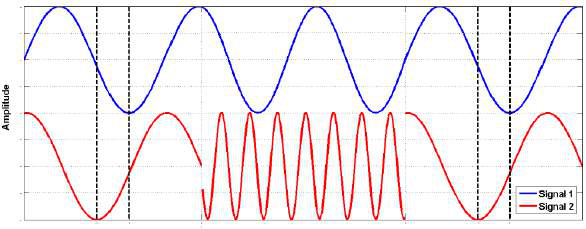
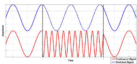
Figure 15: Phase-Coherent Switching. The relative phase between channels 1 and 2 remains the same after channel 2 temporarily switched to a different frequency.Figure 16: Phase Memory. The signal returns to the same absolute phase when returning to the previous frequency and amplitude setting.
Mode
Description
Remarks
Phase coherent switching2 (Multi-channel mode)
Phase coherent switching guarantees deterministic and reproducible phase relationships between multiple individual channels across multiple individual units.
Option PHS
Phase coherent switching2 (Multi-device mode)
Also enables synchronous playback of I/Q waveforms on multiple channels and multiple devices.
Options SYNC + PHS
Phase Memory
With phase memory the RF output phase behaves as if switching between individual, continuously running RF sources.
Option PHS
Phase calibratable mode
Combinations of phase correction and calibratable mode are available. Phase correction off / calibratable off (default): channel-to-channel relative phases are stable and repeatable, but not zero and vary over power and frequency. Phase correction off / calibratable on: linear relative phase variation over frequency and static phase over power. Phase correction on / calibratable on: correction values interpolated between points, enabling true zero phase offset between channels over any frequency/power range (up to a device's full power and frequency range).
Option PCM
2 Limitations: as the synthesized signal undergoes further routing and amplitude control (filtering and amplitude control), it is subject to electrical delays before reaching the RF output. Those delays vary with RF amplitude and frequency but are otherwise stable. The relative phase between channels will not be zero, but is deterministic and reproducible: for any fixed combination of frequency and amplitude settings, the resulting relative phase between channels will always be the same, even over power cycles.
Multi-Channel Performance
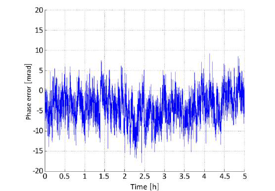
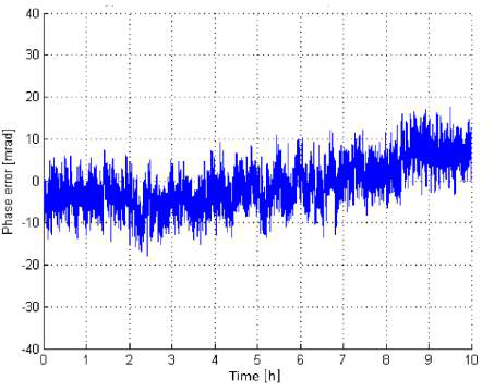
Figure 17: Phase coherence performance at 38 GHz.Figure 18: Phase coherence performance at 15 GHz.Figure 19: 875 typical channel-to-channel phase error, CH1 @0.5 GHz mixed with CH2 @2.5 GHz vs 2 GHz from another device.
Parameter
Typical
Note
Isolation between channels
> 90 dB
Relative Phase Stability
TBD
Trigger Source
Synchronous (initiate and trigger multiple channels)
Additional Delay to Asynchronous Characterizations
1 µs ±100 ns
Channel to Channel Jitter
±10 ps typ.
Multi-Device Performance (Option SYNC)
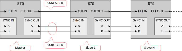
Figure 20: Connections for multi-device synchronization. The reference clock uses SMA connectors (cable and connectors must support at least 6 GHz). Sync signals A, B, C use SMB connectors (at least 3 GHz).
Parameter
Typical
Multi-Device Synchronization
TBD
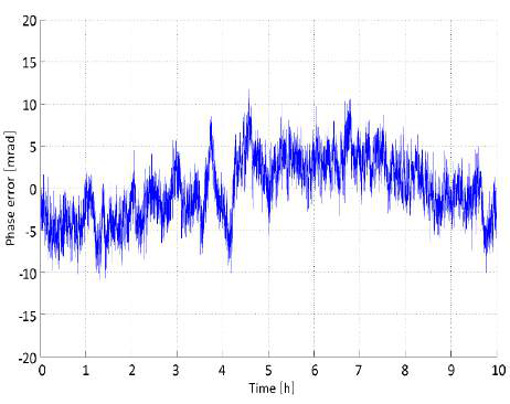
Relative Phase Stability
TBD
11Analog Modulation (Option MOD)
Pulse Modulation
Figures 21–24: Pulsed chirp (10 µs, 400 MHz bandwidth) and pulse modulation (16 ns at 10 GHz and 40 GHz).
Figure 26: Wideband FM (1 MHz rate, 200 MHz deviation).
Parameter
Min
Typical
Max
Note
Modulation Source
Internal
External
Option AIQ
Maximum Frequency Deviation (peak)
200 MHz
Output is clipped at max power level
Deviation Accuracy
0.5%
1%
Distortion (THD)
< 1%
Modulation Frequency Range
0.1 Hz
100 MHz
Modulation Waveforms
Sine
Phase Modulation
Parameter
Min
Typical
Max
Note
Modulation Source
Internal
External
Option AIQ
Phase Deviation (peak)
0
100 rad
Deviation Accuracy
0.5%
1%
Modulation Frequency Range
0.1 Hz
100 MHz
Modulation Waveforms
Sine
Distortion (THD)
< 1%
1 kHz rate & N × rad deviation
12Pulse Descriptor Word (Option PDW)
The PDW is an operating mode of the 875 which takes control of the RF output. Other 875 features cannot be used simultaneously unless their settings are available as PDW parameters. The PDW feature supports several methods for uploading parameters to the device, including PDW list files in .csv format and streaming through FCP.
Parameter
Typical
Note
PDW Format — see App Note AN6008 for PDW details
PDW Mode
List
Stream
Option FCP
PDW Time Mode
Relative, absolute
Controllable Parameters
Start time, pulse width, frequency, power, phase, waveform segment ID
Parameter Range
Full specified range
RF Frequency / RF Phase
-20 to +15 dBm
RF Power
8 ns to 208 d
Start Time
8 ns to 208 d
Pulse Width
Parameter Setting Resolution
1/29 Hz
RF Frequency
1/27 dB
RF Power
0.0055 deg
RF Phase
8 ns
Start Time / Pulse Width
Automatic Level Control (ALC) Mode
OFF
Power Level Uncertainty
0.5 dB (max 1 dB)
875-04
TBD
875-20, 875-40
PDW Timing — see AN6008 for timing details
Switching Time (transient)
500 µs
875-06/12/20/40 Option UFS
TBD (= 20 µs)
875-04 Option UFS & Option PHS
2 µs / 3.2 µs
875-04 Option UFS
Pulse Width
32 ns (min)
8 ns (min)
Option UFS
Play Time
up to 208 d
Absolute Time Mode
Simulation Trigger Setup Time
32 ns
Trigger Parameters
See Trigger Capability
PDW Buffer Size
1 to 1024 PDW
For both PDW modes
PDW List Count
Infinite, 1 to 65 M
Mode Overview
PDW Mode
Input Interface
PDW Upload
Device Storage
Simulation
List
875 GUI / SCPI commands
Before simulation starts
PDW Memory
All PDWs in list, optionally repeat list
Stream
FCP / SCPI commands
Before and during simulation
PDW Buffer (FIFO)
PDWs in order of upload, only once
13I/Q Modulator & Baseband Generator
I/Q Modulator
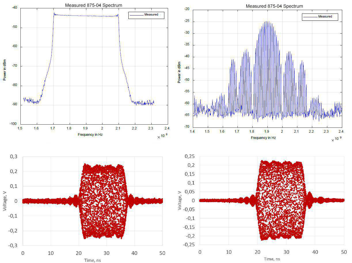
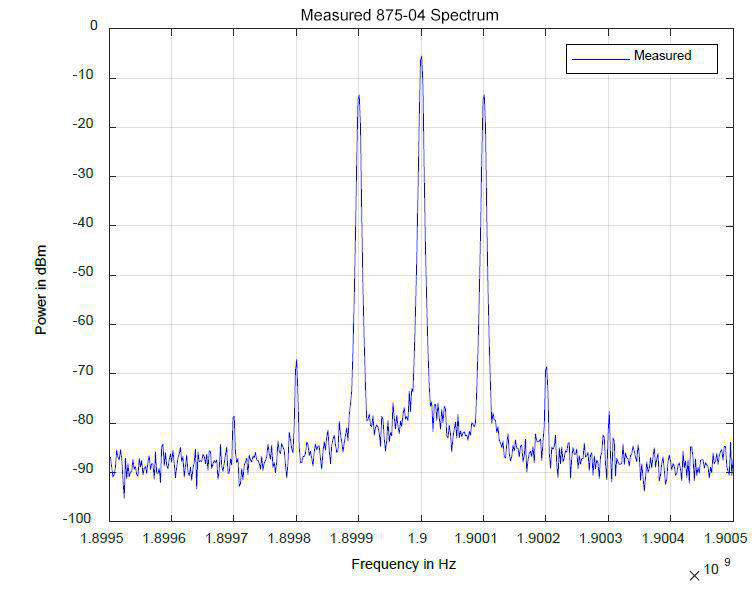
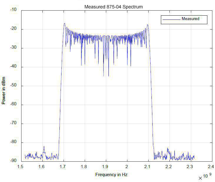
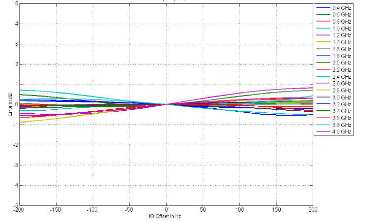
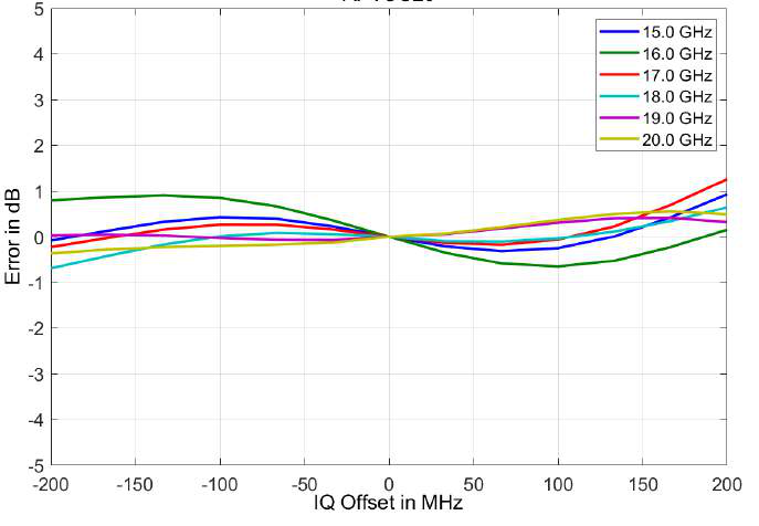
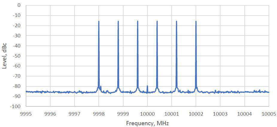
Figure 27: I/Q Relative Response (measured), 875-04.Figure 28: I/Q Relative Response (measured), 875-20.Figure 29: Carrier suppression -80 dBc for 0 dBm 6-tone signal at 10 GHz carrier.
Parameter
Min
Typical
Max
Note
RF Modulation Bandwidth
400 MHz
I/Q Frequency Response over full 400 MHz
±1.0 dB
±1.5 dB
< 6 GHz
±1.5 dB
±2.5 dB
6 to 20 GHz
±2.0 dB
±3.5 dB
20 to 40 GHz
Carrier Leakage
-90 dBc
-70 dBc
Image Sideband Rejection
65 dBc
85 dBc
Internal I/Q Baseband Generator
Parameter
Min
Typical
Max
Note
Sample Resolution
16 bits
Clock Source
Internal
Sample Rate
10 Hz
500 MHz
Sample Rate Resolution
1 Hz
Waveform Length (number of samples)
96*
512 M
246*
334 M
Marker signals active
Segment Mode
Number of Segments
1
65 k
Segment Changeover
Seamless, immediate
Trigger Modes
Same segment, next segment, addressed segment
Sequencer Play List Length
1
2048
Sequence Segment Repetitions
1
10 M
Changeover Time
2 µs
500 MHz sample rate, after trigger event, immediate changeover
Arbitrary Trigger
Trigger Type
Normal, next segment, next sequence
Check with BNC support
Trigger Parameters
See Trigger Capability
External Trigger Event to RF Output Delay
0.5 µs ±100 ns
500 MHz sample rate
Marker Signals (defined during waveform generation)
Number of Markers
4
Type
Waveform
Marker Delay Setting Range / Resolution
TBD
Marker Duration Minimum Value
1 sample
Sample rate ≤ 125 MHz
4 samples
Sample rate ≥ 125 MHz
Marker Duration Variation
±1 sample
Sample rate ≤ 125 MHz
±8 ns
Sample rate ≥ 125 MHz
Marker Jitter
±1 sample
Sample rate ≤ 125 MHz
±8 ns
Sample rate ≥ 125 MHz
Marker Polarity
Normal, inverted
Marker Output to RF Output Delay
TBD
* Shorter waveforms will be automatically extended by cyclically repeating the waveform.
14Vector & Multicarrier Generation
Internal Vector Modulation (Option IVM)
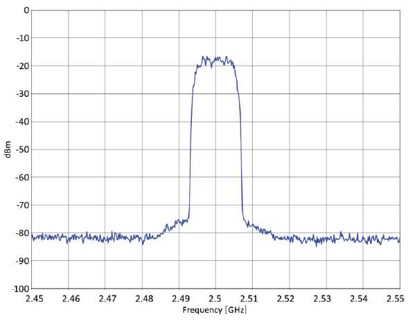
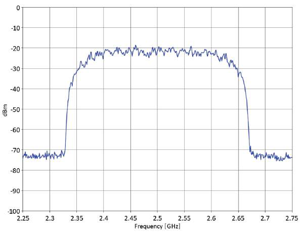
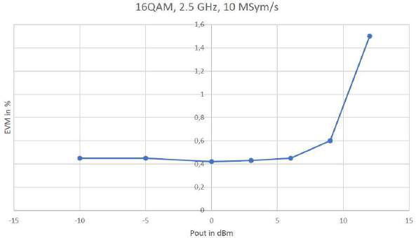
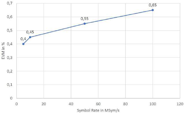
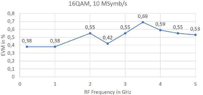
Figure 30: 256QAM, 10 MS/s.Figure 31: 16QAM, 250 MS/s.Figure 32: EVM vs. Output Power, 16QAM, 10 MS/s, 2.5 GHz.Figure 33: EVM vs. Symbol Rate, 16QAM.Figure 34: EVM vs. RF Frequency, 16QAM, 10 MSymbols/s.
FM Component (nominal 30 Hz navigation reference signal)
FM Index
0
33.3
FM Index Resolution
0.01
FM Index Accuracy
±0.033
FM Deviation Accuracy 480 Hz
1 Hz
Identification Code Component (4-character code)
State
On/Off
AM Frequency
300 Hz
1740 Hz
AM Frequency Resolution
0.1 Hz
AM Frequency Accuracy
±1 mHz
AM Depth
0
50%
AM Depth Resolution
0.01%
AM Depth Accuracy
±0.5%
ILS Modulation
Generation of ILS Localizer (ILS-LOC) and ILS Glideslope (ILS-GS) signals.
Parameter
Min
Typical
Max
Note
ILS LOC
Frequency Range
108 MHz
118 MHz
Carrier frequency range
DDM Range
-193.5 µA
+193.5 µA
DDM Resolution
0.1 µA
DDM Accuracy
±4.8 µA
SDM Range
20%
60%
SDM Resolution
0.01%
SDM Accuracy
±1%
AM0 Component (nominal 90 Hz beam)
Beam State
On/Off
AM0 Depth (change DDM/SDM)
10%
30%
AM0 Depth Resolution
0.01%
AM0 Depth Accuracy
±0.5%
Frequency
88 Hz
92 Hz
Frequency Resolution
0.0005 Hz
Frequency Accuracy
±500 µHz
AM1 Component (nominal 150 Hz beam)
Beam State
On/Off
AM1 Depth (change DDM/SDM)
10%
30%
AM1 Depth Resolution
0.01%
AM Depth Accuracy
±0.5%
Frequency
147 Hz
154 Hz
Frequency Resolution
0.0005 Hz
Frequency Accuracy
±500 µHz
Range of Relative Phase to AM0 Component
0
360°
Resolution of Relative Phase to AM0 Component
0.001
Accuracy of Relative Phase to AM0 Component
±1°
Identification Code Component (4-character code)
Identification State
On/Off
AM Frequency
300 Hz
1740 Hz
AM Frequency Resolution
0.0005 Hz
AM Frequency Accuracy
±500 µHz
AM Depth
0
50%
AM Depth Resolution
0.01%
AM Depth Accuracy
±0.5%
ILS GS
Frequency Range
329 MHz
335 MHz
Carrier frequency range
DDM Range
-342.8 µA
+342.8 µA
DDM Resolution
0.1 µA
DDM Accuracy
±4.8 µA
SDM Range
40%
120%
SDM Resolution
0.01%
SDM Accuracy
±1%
AM0 Component (nominal 90 Hz upper beam)
Beam State
On/Off
AM0 Depth (change DDM/SDM)
20%
60%
AM0 Depth Resolution
0.01%
AM Depth Accuracy
±0.5%
Frequency
88 Hz
92 Hz
Frequency Resolution
0.0005 Hz
Frequency Accuracy
±500 µHz
AM1 Component (nominal 150 Hz lower beam)
Beam State
On/Off
AM1 Depth (change DDM/SDM)
20%
60%
AM1 Depth Resolution
0.01%
AM Depth Accuracy
±0.5%
Frequency
147 Hz
154 Hz
Frequency Resolution
0.0005 Hz
Frequency Accuracy
±500 µHz
Range of Relative Phase to AM0 Component
0
360°
Resolution of Relative Phase to AM0 Component
0.001
Accuracy of Relative Phase to AM0 Component
±1°
Marker Beacon
Parameter
Typical
Note
AM Tone Accuracy (95% AM)
5% of setting
AM Tone Distortion (95% AM)
5%
16Additive White Gaussian Noise (Option AWGN)
Parameter
Typical
Min
Max
Note
Noise
Distribution Density
Gaussian, statistical, μ = 0, σ2 = 1
Separate for I and Q
Crest Factor
≤ 21.07 dB
Depending on C/N ratio
Periodicity
> 7×1044 s
Carrier to Noise Ratio C/N
Range
-60 dB
90 dB
Limited by the RF output power
Resolution
0.01 dB
See application note AN6005
Noise Bandwidth
Dependency
0.8 of I/Q baseband generator sample rate / manually
Any modulation active / all modulations inactive
Range
10 Hz
400 MHz
Resolution
1 Hz
Power Control Mode
Total, carrier, noise
17Triggers & Multi-Function I/O
Trigger Capability
Parameter
Min
Typical
Max
Note
Trigger Mode
Single, continuous
Trigger Source
Internal (immediate, bus), external
External Trigger Input
Connector Type
MF1 IN, MF2 IN
See External Multi-Function Inputs
Delay Setting Range
0 s
8.5 s
Delay Setting Resolution
2 ns
Jitter
±2 ns
Slope
Rising, falling
Trigger Output
Connector Type
MF1 OUT, MF2 OUT
See External Multi-Function Outputs
Polarity
Normal, inverted
Delay Setting Range
0 s
2 µs
Delay Setting Resolution
2 ns
Pulse Width Setting Range
8 ns
16 µs
Pulse Width Setting Resolution
8 ns
External Multi-Function Inputs
Parameter
Min
Typical
Max
Note
Connector
MF1 IN, MF2 IN
See Connectors
Application
External pulse modulation, external trigger
Nominal Input Impedance
DC 10 kΩ and AC 50 Ω
Threshold Voltage
0.85 V
0.9 V
0.95 V
Nominal Input Voltage
0 V
3.3 V
TTL compatible
Hysteresis
60 mV
External Multi-Function Outputs
Parameter
Min
Typical
Max
Note
Connector
MF1 OUT, MF2 OUT
See Connectors
Application
Pulse video signal, trigger, marker signals (1–4)
Nominal Output Impedance
TBD
Nominal Output Voltage
0 V
3.3 V
LVTTL
18Fast Control Port, Analog Inputs & SD Card
Fast Control Port (Option FCP)
Parameter
Value / Note
Interface
Parallel, bidirectional LVDS with 100 Ω termination at receiver
Common Mode Level
Typ. 1.2 V
Differential Input Threshold
Typ. ±100 mV
Differential Output Voltage
Typ. 300 mV
Connector
FCP I/O — see Connectors
Mode: I/Q Data Streaming
Sample Rate
125 and 250 MHz
Input/Output Format
Data (16 bits), clock signal, valid signal
Valid I/Q Data Input to RF Output Delay
Typ. TBD ns
Mode: Segment ID Streaming
Input Format
Data (16 bits), valid signal (signal must be static low or high)
Valid Segment ID Input to RF Output Delay (immediate segment changeover)
Typ. TBD ns
Valid Segment ID Jitter
±8 ns
Mode: CDW Streaming — 875-04 Option FCP & UFS. CDW is an operating mode of the 875 which takes control of the RF output. Other 875 features cannot be used simultaneously unless their settings are available as CDW parameters.
Parameter
Frequency (up to 48 bit), power, phase, segment ID
Parameter Range and Resolution
See Pulse Descriptor Word
Input Format
Address (8 bits), data (8 bits), valid signal
Sampling Rate
250 MHz
Valid Signal Level Min. Period
8 ns
Data to Valid Setup and Hold Time
4 ns
Automatic Level Control (ALC) Mode
OFF
External Analog Inputs (Option AIQ)
Parameter
Min
Typical
Max
Note
Connector
I IN, Q IN
See Connectors
Analog Bandwidth
50 MHz
Maximum Input Voltage
-2 V
+2 V
Nominal Input Voltage Range
±0.5 V
90%
Input Impedance
50 Ω
Additional Features
Individual gain and DC offset adjustment, overrange detection
Application
Analog I/Q data modulation, external AM, FM, PM modulation
Option AIQ / Option AIQ & MOD
SD Card (Option SD)
Type
Support
SD
Up to 2 GB with FAT 12 or FAT 16
SDHC
Up to 32 GB with FAT 32
19Connectors
Single Channel Model
Front Panel
Label
Type
Description
Option / Model
RF 50 Ω
Type N Female
RF output
875-04 / -06 / -12
SMA Female
RF output
875-20
K (2.92 mm) Female
RF output
875-40
Rear Panel
Label
Type
Description
Option
DC24V
DC power plug, female
Power of instrument
M4
Ground reference screw
USB
USB type B
Remote programming interface
LAN
RJ-45
Remote programming interface
CLK IN
SMA, female
High-stability reference input
SYNC
CLK OUT
SMA, female
High-stability reference output
SYNC
SYNC IN, SYNC OUT
SMB, male
Multi-device synchronization ports
SYNC
SD
MicroSD
Card slot for non-volatile storage of I/Q data
REF IN
BNC female
Reference frequency input
REF OUT
BNC female
Reference frequency output
MF1 IN, MF2 IN
SMB male
Multi-function digital inputs (user-configurable)
MF1 OUT, MF2 OUT
SMB male
Multi-function digital outputs (user-configurable)
I IN, Q IN
BNC female
Analog inputs (user-configurable)
AIQ
FCP
36-pin mini-D female / 3M MDR 102 Series
Fast control port, external digital I/Q data streaming (per channel)
FCP
2U Multi-Channel Model
Front Panel
Label
Type
Description
Model
RF OUT (per channel)
SMA Female
RF output
875-20-X
K (2.92 mm) Female
RF output
875-40-X
Rear Panel
Label
Type
Description
Option
C13
Power of instrument
M4
Ground reference screw (earth)
USB
USB type B
Remote programming interface
LAN
RJ-45
Remote programming interface
GPIB
24-pin female
Remote programming interface
SD
MicroSD
Card slot for non-volatile storage of I/Q data
REF IN
BNC female
Reference frequency input
REF OUT
BNC female
Reference frequency output
CLK IN
SMA female
High-stability reference input
SYNC
CLK OUT
SMA female
High-stability reference output
SYNC
FCP (per channel)
36-pin mini-D female / 3M MDR 102 Series
Fast control port
FCP
MF1 IN, MF2 IN (per channel)
SMB male
Multi-function inputs (user-configurable)
MF1 OUT, MF2 OUT (per channel)
SMB male
Multi-function outputs (user-configurable)
I IN, Q IN (per channel)
SMB male
Analog inputs (user-configurable)
AIQ
SYNC IN, SYNC OUT
SMB, male
Multi-device synchronization ports
SYNC
20Ordering Information
Host Models
Host Model
Product
Description
875 — single channel model
875-04
4 GHz model
875-06
6 GHz model
875-12
12 GHz model
875-20
20 GHz model
875-40
40 GHz model
875-X — 2U rack-mount model -X: channels = (1), 2, 3 or 4
875-04-X
4 GHz model
875-06-X
6 GHz model
875-12-X
12 GHz model
875-20-X
20 GHz model
875-40-X
40 GHz model
Hardware Options
Applicability
Product
Description
875(-X)
Option LN
Enhanced close-in phase noise & frequency stability
875(-X)
Option LN+
Enhanced close-in phase noise & further enhanced long-term frequency stability
875(-X)
Option SYNC
Multi-device synchronization ports
875(-X)
Option FCP
Fast control port, external digital I/Q data streaming (per channel)
Firmware for Phase Calibratable Mode (per channel), option PHS required
875(-X)
Option PDW
Pulse descriptor word (per channel)
875(-X)
Option MOD
Internal analog modulations
875(-X)
Option IVM
Internal digital modulation schemes (per channel)
875(-X)
Option AVIO
Internal avionics modulations (per channel)
875(-X)
Option AWGN
Additive white Gaussian noise generator (per channel)
875(-X)
Option SD
MicroSD card support for non-volatile storage of I/Q data
875(-X)
Option VREF
Variable external reference
Accessories
Applicability
Product
Description
875
Option EB
External battery with adapter cable
For a configured quote, contact Berkeley Nucleonics Corporation · info@berkeleynucleonics.com · 415-453-9955.
21General Characteristics
Remote Programming Interfaces
Characteristic
Specification
Interfaces
Ethernet 100BaseT LAN interface; USB 2.0 device interface; GPIB (IEEE-488.2, 1987) with listen and talk (Option GPIB)
Control language
SCPI version 1999.0
Power Requirements — Single Channel Model
Parameter
Value
Note
Input Voltage Range
24 VDC ±3.0 V
Power Consumption (typ, without options)
45 W
875-04
65 W
875-06 to 875-40
Main Adapter Supplied (without options)
100–240 VAC 50/60 Hz; 24 VDC, 65 W max
875-04
100–240 VAC 50/60 Hz; 24 VDC, 160 W max
875-06 to 875-40
Power Requirements — Multi-Channel Model
Parameter
Value
Note
Input Voltage Range
100–240 VAC 50/60 Hz
Fuse Rating
5×20 mm, 250 V, 6.3 AT
2-poles, each
Power Consumption (max)
200 W
875-04-X, 875-06-X, 875-12-2, 875-20-2, 875-40-2
400 W
875-06-2, 875-12-04, 875-20-4, 875-40-4
Environmental
Characteristic
Specification
Environmental
Levels similar to MIL-PRF-28800F Class 3/4. Samples of this product have been type tested to be robust against the environmental stresses of storage, transportation, and end-use (temperature, humidity, shock, vibration, altitude, and power line conditions).
Operating temperature range
0 to 45 °C
Storage temperature range
-40 to 70 °C
Operating and storage altitude
Up to 15,000 feet (4600 m)
EMC
Complies with EMC regulations and directives for emission and immunity to interference (EN 61326-1 Industrial, EN/IEC 61326-2-1)
Safety
Complies with applicable safety regulation IEC/EN 61010-1
RoHS
Complies with directive 2011/65/EU
Recommended calibration cycle
24 months
Physical — Single Channel (portable / benchtop)
Characteristic
Specification
Weight
6 lbs [2.7 kg] to 9.7 lbs [4.4 kg] net, without main adapter
Dimensions (incl. rubber)
4.88 in H × 7.17 in W × 11.85 in L [124 mm H × 182 mm W × 301 mm L]
Dimensions (with RF output connector type N)
4.88 in H × 7.17 in W × 12.20 in L [124 mm H × 182 mm W × 310 mm L]